- 您现在的位置:买卖IC网 > Sheet目录369 > W971GG8JB-25 (Winbond Electronics)IC DDR2 SDRAM 1GBIT 60WBGA
�� �
�
�W971GG8JB�
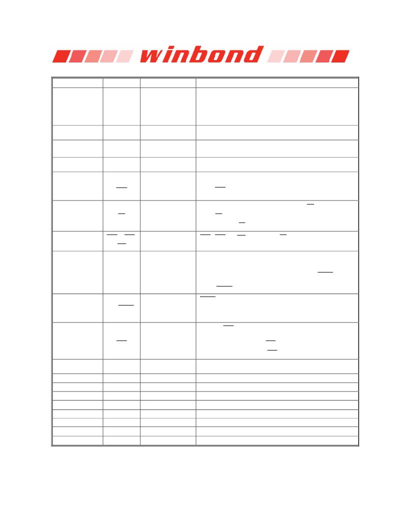
�6.� BALL� DESCRIPTION�
�BALL� NUMBER�
�SYMBOL�
�FUNCTION�
�DESCRIPTION�
�Provide� the� row� address� for� active� commands,� and� the� column�
�H8,H3,H7,J2,J8,J3,�
�J7,K2,K8,K3,H2,K7,�
�L2,L8�
�A0� ?� A13�
�Address�
�address� and� Auto-precharge� bit� for� Read/Write� commands� to� select�
�one� location� out� of� the� memory� array� in� the� respective� bank.�
�Row� address:� A0� ?� A13.�
�Column� address:� A0� ?� A9.� (A10� is� used� for� Auto-precharge)�
�G2,G3,G1�
�C8,C2,D7,D3,D1,D9,�
�B1,B9�
�F9�
�B7,A8�
�BA0� ?� BA2�
�DQ0� ?� DQ7�
�ODT�
�DQS,�
�DQS�
�Bank� Select�
�Data� Input�
�/� Output�
�On� Die� Termination�
�Control�
�Data� Strobe� /�
�Differential� Read� Data�
�Strobe�
�BA0� ?� BA2� define� to� which� bank� an� ACTIVE,� READ,� WRITE� or�
�PRECHARGE� command� is� being� applied.�
�Bi-directional� data� bus.�
�ODT� (registered� HIGH)� enables� termination� resistance� internal� to�
�the� DDR2� SDRAM.�
�Output� with� read� data,� input� with� write� data� for� source� synchronous�
�operation.� Edge-aligned� with� read� data,� center-aligned� with� write�
�data.� DQS� is� only� used� when� differential� data� strobe� mode� is�
�enabled� via� the� control� bit� at� EMR� (1)� [A10]� =� 0.�
�All�
�commands�
�are�
�masked�
�when�
�CS�
�is�
�registered�
�G8�
�CS�
�Chip� Select�
�HIGH� .� CS� provides� for� external� Rank� selection� on� systems� with�
�multiple� Ranks.� CS� is� considered� part� of� the� command� code.�
�F7,G7,F3�
�RAS� ,� CAS� ,�
�WE�
�Command� Inputs�
�RAS� ,� CAS� and� WE� (along� with� CS� )� define� the� command� being�
�entered.�
�DM� is� an� input� mask� signal� for� write� data.� Input� data� is� masked�
�when� DM� is� sampled� HIGH� coincident� with� that� input� data� during� a�
�B3�
�DM/RDQS�
�Input� Data� Mask/�
�Read� Data� Strobe�
�Write� access.� DM� is� sampled� on� both� edges� of� DQS.� The� DM�
�loading� matches� the� DQ� and� DQS� loading.� RDQS/� RDQS� are� used�
�as� strobe� signals� during� reads� is� enabled� by� EMR� (1)� [A11]� =� 1.� If�
�RDQS/� RDQS� is� enabled,� the� DM� function� is� disabled.�
�RDQS� is� only� used� when� RDQS� is� enabled� and� differential� data�
�A2�
�NU/� RDQS�
�Not� Use/Differential�
�Read� Data� Strobe�
�strobe� mode� is� enabled.� If� differential� data� strobe� mode� is� disabled�
�via� the� control� bit� at� EMR� (1)� [A10]� =� 1,� then� ball� A2� and� A8� are� not�
�used.�
�CLK� and� CLK� are� differential� clock� inputs.� All� address� and� control�
�E8,F8�
�CLK� ,�
�CLK�
�Differential� Clock�
�Inputs�
�input� signals� are� sampled� on� the� crossing� of� the� positive� edge� of�
�CLK� and� negative� edge� of� CLK� .� Output� (read)� data� is� referenced�
�to� the� crossings� of� CLK� and� CLK� (both� directions� of� crossing).�
�F2�
�E2�
�A1,E9,H9,L1�
�A3,E3,J1,K9�
�A9,C1,C3,C7,C9�
�A7,B2,B8,D2,D8�
�L3,L7�
�E1�
�E7�
�CKE�
�V� REF�
�V� DD�
�V� SS�
�V� DDQ�
�V� SSQ�
�NC�
�V� DDL�
�V� SSDL�
�Clock� Enable�
�Reference� Voltage�
�Power� Supply�
�Ground�
�DQ� Power� Supply�
�DQ� Ground�
�No� Connection�
�DLL� Power� Supply�
�DLL� Ground�
�CKE� (registered� HIGH)� activates� and� CKE� (registered� LOW)�
�deactivates� clocking� circuitry� on� the� DDR2� SDRAM.�
�V� REF� is� reference� voltage� for� inputs.�
�Power� Supply:� 1.8V� ?� 0.1V.�
�Ground.�
�DQ� Power� Supply:� 1.8V� ?� 0.1V.�
�DQ� Ground.� Isolated� on� the� device� for� improved� noise� immunity.�
�No� connection.�
�DLL� Power� Supply:� 1.8V� ?� 0.1V.�
�DLL� Ground.�
�Publication� Release� Date:� Jun.� 15,� 2012�
�-7-�
�Revision� A02�
�发布紧急采购,3分钟左右您将得到回复。
相关PDF资料
W9725G6IB-25
IC DDR2-800 SDRAM 256MB 84-WBGA
W9725G6JB25I
IC DDR2 SDRAM 256MBIT 84WBGA
W9725G6KB-25I
IC DDR2 SDRAM 256MBIT 84WBGA
W972GG6JB-3I
IC DDR2 SDRAM 2GBITS 84WBGA
W9751G6IB-25
IC DDR2-800 SDRAM 512MB 84-WBGA
W9751G6KB-25
IC DDR2 SDRAM 512MBIT 84WBGA
W9812G6JH-6I
IC SDRAM 128MBIT 54TSOPII
W9816G6IH-6I
IC SDRAM 16MBIT 50TSOPII
相关代理商/技术参数
W9725G6IB-25
功能描述:IC DDR2-800 SDRAM 256MB 84-WBGA RoHS:是 类别:集成电路 (IC) >> 存储器 系列:- 标准包装:1,000 系列:- 格式 - 存储器:EEPROMs - 串行 存储器类型:EEPROM 存储容量:4K (512 x 8) 速度:400kHz 接口:I²C,2 线串口 电源电压:2.7 V ~ 5.5 V 工作温度:-40°C ~ 85°C 封装/外壳:8-SOIC(0.173",4.40mm 宽) 供应商设备封装:8-MFP 包装:带卷 (TR)
W9725G6JB
制造商:WINBOND 制造商全称:Winbond 功能描述:4M ? 4 BANKS ? 16 BIT DDR2 SDRAM
W9725G6JB-25
制造商:Winbond Electronics Corp 功能描述:DRAM Chip DDR2 SDRAM 256M-Bit 16Mx16 1.8V 84-Pin WBGA 制造商:Winbond Electronics 功能描述:512MB DDRII
W9725G6JB25I
功能描述:IC DDR2 SDRAM 256MBIT 84WBGA RoHS:是 类别:集成电路 (IC) >> 存储器 系列:- 标准包装:150 系列:- 格式 - 存储器:EEPROMs - 串行 存储器类型:EEPROM 存储容量:4K (2 x 256 x 8) 速度:400kHz 接口:I²C,2 线串口 电源电压:2.5 V ~ 5.5 V 工作温度:-40°C ~ 85°C 封装/外壳:8-VFDFN 裸露焊盘 供应商设备封装:8-DFN(2x3) 包装:管件 产品目录页面:1445 (CN2011-ZH PDF)
W9725G6KB-18
制造商:Winbond Electronics 功能描述:IC MEMORY 制造商:Winbond Electronics Corp 功能描述:IC MEMORY
W9725G6KB-25
功能描述:IC DDR2 SDRAM 256MBIT 84WBGA RoHS:是 类别:集成电路 (IC) >> 存储器 系列:- 标准包装:1 系列:- 格式 - 存储器:闪存 存储器类型:闪存 - NAND 存储容量:4G(256M x 16) 速度:- 接口:并联 电源电压:2.7 V ~ 3.6 V 工作温度:0°C ~ 70°C 封装/外壳:48-TFSOP(0.724",18.40mm 宽) 供应商设备封装:48-TSOP I 包装:Digi-Reel® 其它名称:557-1461-6
W9725G6KB-25 TR
制造商:Winbond Electronics Corp 功能描述:256M DDR2-800, X16
W9725G6KB25A
制造商:WINBOND 制造商全称:Winbond 功能描述:DLL aligns DQ and DQS transitions with clock, Data masks (DM) for write data, Write Data Mask